

Market Analysis By Advanced Smart Product PCBA Factory On The Growth Of Next-Gen Smart Electronics

Global demand for next-generation smart electronics accelerates at a rapid pace. Modern hardware ecosystems depend heavily on real-time local processing, robust connectivity, and intelligent automation. Consequently, fields like Artificial Intelligence of Things (AIoT), decentralized edge computing, and ultra-compact wearable devices expand continuously. This digital evolution transforms consumer expectations, forcing original equipment manufacturers to rethink traditional electronic hardware architectures. To address these shifts, brand owners rely on an Advanced Smart Product PCBA Factory to bridge the gap between complex software designs and physical hardware realities. Hardware engineering groups face the immense challenge of accommodating vast processing capabilities within highly restricted dimensions.
The rapid rise of edge computing creates a unique manufacturing dilemma for product developers worldwide. Localized edge systems require immediate data processing capabilities directly at the device level. As a result, product layouts must incorporate advanced microcontrollers, high-speed memory modules, and multi-protocol radio frequency components simultaneously. This concentration of complex silicon chips creates severe physical spatial challenges on the underlying printed circuit board. Traditional circuit layout methodologies fail to support these dense configurations because component spacing has shrunk past conventional limits. When high-frequency modules operate in close proximity, localized electromagnetic interference and thermal crowding become common problems. Navigating these multi-layered spatial constraints demands innovative assembly techniques that prevent functional degradation during deployment.
Furthermore, next-generation wearable technologies amplify these physical packaging complications. Modern consumers demand sleeker, smaller, and more ergonomic smart wearables that track multiple bio-metrics concurrently. To satisfy these market desires, engineers must integrate optical sensors, power management systems, and battery protection circuits onto irregularly shaped substrates. This geometric complexity completely eliminates the luxury of utilizing flat, spacious circuit boards. Miscalculating structural trace tolerances or component placement risks total device failure or severe signal cross-talk. Consequently, the international smart device sector requires an analytical engineering approach to production rather than simple assembly execution. Resolving these dimensional bottlenecks determines whether a concept scales successfully in competitive global markets.
Breaking the Micro-Scale Barrier: The Crucial Role of Advanced FPC SMT and SiP Assembly in Product Evolution
Overcoming extreme spatial limitations requires a fundamental transition toward specialized manufacturing processes. Flexible Printed Circuit (FPC) surface mount technology offers a viable solution for complex, space-constrained enclosures. FPC materials allow the circuit board to bend, fold, and twist inside non-linear product housings without breaking electrical connections. However, handling ultra-thin flexible substrates during high-speed pick-and-place routines introduces mechanical vulnerabilities. Because these materials lack structural rigidity, minor tension variations during printing or component placement can warp traces. Elite electronic manufacturing partners resolve this by developing specialized vacuum tooling fixtures and precision tension controls to stabilize flexible materials during reflow.
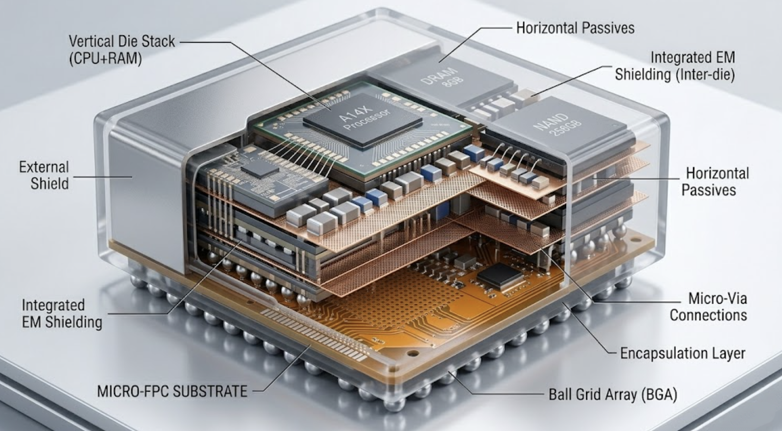
Simultaneously, System-in-Package (SiP) micro-integration redefines how engineers design high-density smart devices. Traditional Surface Mount Technology (SMT) spreads discrete components horizontally across a wide planar area. In contrast, SiP architecture stacks multiple heterogeneous semiconductor dies, passives, and shielding components both horizontally and vertically inside a single compact module. This advanced encapsulation effectively condenses an entire functional subsystem into the footprint of an individual chip. By reducing physical distances between processing cores and memory arrays, SiP architecture drastically improves signal propagation speeds. Moreover, integrated shielding within SiP modules mitigates electromagnetic interference, satisfying the consumer preference for smaller device profiles.
This technical evolution provides a direct upgrade pathway for premium consumer electronics and specialized industrial systems. By leveraging advanced assembly methods, companies deploy complex algorithms on miniaturized hardware without sacrificing battery life or thermal efficiency. Physical consolidation directly shortens trace lengths, lowering parasitic capacitance and inductance. Consequently, smart devices achieve higher operational frequencies while consuming less power during peak computational cycles. For global technology brands, adopting these advanced packaging methods remains a core necessity to maintain long-term market relevance and secure consumer loyalty in saturated markets.
Beyond Simple Assembly: Eliminating Structural Bottlenecks Through Rigorous Pre-Production DFM
As component densities reach microscopic levels, the margins for manufacturing errors disappear entirely. Minor trace layout imperfections can lead to catastrophic structural defects during mass production. For example, uneven thermal absorption across dense component arrays often causes component tombstoning, where tiny components lift off their pads during reflow. Furthermore, tightly packed pin-grid arrays increase the likelihood of microscopic solder bridging, causing hidden short circuits beneath components. To prevent these costly setbacks, sophisticated facilities implement exhaustive Design for Manufacturability (DFM) verification protocols. This pre-production evaluation acts as a predictive shield, identifying layout errors and thermal mismatch risks before factory tooling begins.
Moreover, rigorous DFM processes prove invaluable for high-reliability applications, such as a one-stop turnkey PCBA solution for automotive electronics and new energy vehicles. Automotive environments subject electronic controls to intense vibrations, temperature swings, and severe environmental exposure. A failure in an electric vehicle power module can compromise user safety and trigger costly product recalls. Therefore, DFM engineers meticulously analyze copper weight distributions, solder mask definitions, and thermal via placements to guarantee long-term joint integrity under harsh conditions. Ensuring uniform thermal dissipation prevents localized hot spots from degrading delicate semiconductor structures over time, bridging the gap between raw design and long-term reliability.
Ultimately, proactive yield optimization eliminates the inefficient cycle of post-production debugging. Traditional manufacturing relies heavily on finding defects after assembly, which wastes valuable materials and extends development timelines. Shifting engineering scrutiny to the digital pre-production phase protects project budgets and ensures predictable manufacturing outcomes. This systematic review ensures that multi-layer printed circuit boards transition smoothly from prototype stages to automated mass production. Consequently, technology enterprises launch complex hardware platforms with absolute confidence in their structural integrity, operational longevity, and market-readiness.
Bridging Vision and Scalability: How Shenzhen Aozite Technology Secures the Growth Matrix of Smart Electronics
Translating complex next-generation electronic designs into reliable, scalable market realities requires an elite manufacturing partner. Aozite OST PCBA addresses these strict industrial demands by providing complete, high-precision turnkey manufacturing solutions. The enterprise manages the entire hardware deployment process, including advanced material procurement, strict component authentication, and high-speed surface mount assembly. Operating from an expansive, modern production facility, Shenzhen Aozite Technology Co.,Limited operates eight fully automated SMT production lines configured for maximum precision. This state-of-the-art infrastructure delivers a daily capacity exceeding 1.2 million solder joints, allowing global smart product innovators to scale up production seamlessly without experiencing supply delays.
To achieve consistent quality at this massive scale, the internal engineering department conducts deep structural DFM assessments during initial project onboarding. Catching pad mismatches and clearance limitations early ensures smooth transitions during automated high-speed component placement. Furthermore, quality assurance teams at Aozite OST PCBA(Shenzhen Aozite Technology Co., Limited) utilize a multi-layered inspection matrix to monitor production. Advanced 3D Solder Paste Inspection (SPI) systems measure the exact volume and alignment of deposited solder before component placement. Following reflow, automated optical inspection (AOI) units check component orientation at high speeds. Finally, specialized X-ray equipment scans beneath Ball Grid Array (BGA) and SiP modules to verify internal structural bonds, blocking hidden flaws from reaching final products.
By blending advanced quality tracking with open supply chain tracking, the manufacturer effectively minimizes technical risks for international innovators. This rigorous hardware execution enables global technology pioneers to focus entirely on software refinement and market expansion. The combined strength of high-precision machinery, strict engineering verification, and efficient component logistics ensures that complex electronic devices enter the market on schedule. For enterprises aiming to dominate the evolving smart electronics sector, this robust manufacturing foundation provides the necessary predictability, scalability, and quality to achieve lasting commercial success across diverse regional landscapes.
For detailed information regarding advanced smart product assembly capabilities, please visit the official corporate portal: https://www.aozite-pcba.com/.
Aozite OST PCBA
Aozite OST PCBA
Legal Disclaimer:
EIN Presswire provides this news content "as is" without warranty of any kind. We do not accept any responsibility or liability for the accuracy, content, images, videos, licenses, completeness, legality, or reliability of the information contained in this article. If you have any complaints or copyright issues related to this article, kindly contact the author above.
